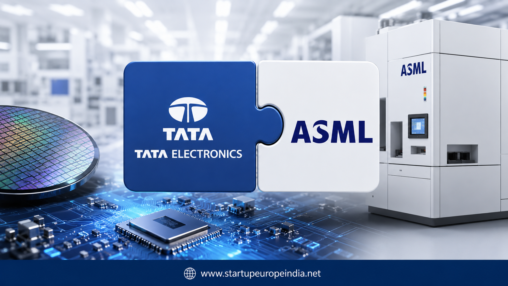
On May 16, 2026, Tata Electronics and ASML signed a Memorandum of Understanding to set up India's first commercial 300mm semiconductor fabrication plant in Dholera, Gujarat. The signing took place during Indian Prime Minister Narendra Modi's visit to the Netherlands, with Dutch Prime Minister Dick Schoof also present, reflecting the diplomatic weight both governments are placing on the deal.
The partnership is significant because ASML is considered one of the most critical companies in the global semiconductor industry. The Dutch company manufactures advanced lithography machines used to produce semiconductor chips. Major chipmakers such as TSMC, Intel, and Samsung rely on ASML equipment for chip manufacturing.
Under the agreement, ASML will deploy its suite of lithography tools and solutions to enable the establishment and ramp-up of the Dholera fab, covering talent development, lithography-intensive skill development, and proactive supply chain resilience. The companies will also develop R&D infrastructure to support the long-term success of the facility.
The Specific Technology Involved
This is where the headline needs grounding. Both TSMC's cutting-edge 2nm fabs and the Dholera facility use 300mm wafers, but the real metric defining a chip's capability is the process node. The Dholera fab will operate at 28nm to 110nm nodes, using ASML's DUV (Deep Ultraviolet) lithography tools, not the more advanced EUV systems used for sub-10nm production.
The specific nodes covered are 28nm, 40nm, 55nm, 90nm, and 110nm, according to the ASML press release, with process technology licensed from Taiwan's Powerchip Semiconductor Manufacturing Corporation (PSMC).
ASML's most sophisticated tools, used for producing 3nm and 5nm chips globally, remain outside the immediate scope. The partnership instead lays groundwork for potential future upgrades.
Production Targets and Chip Types
At full capacity, the fab will produce up to 50,000 wafers per month, manufacturing power management ICs, display drivers, microcontrollers, and high-performance computing chips for automotive, computing and data storage, wireless communications, and AI applications.
Initial commercial production is scheduled for late 2026, which is an aggressive timeline for a greenfield semiconductor project, requiring seamless coordination between construction, equipment installation, and testing. Throughout 2026, ASML tools will be installed and calibrated to meet the requirements of the 28nm to 110nm nodes.
The Dholera site was formally designated a Special Economic Zone in April 2026.
The Partnership Stack Behind the Fab
The ASML deal is not a standalone arrangement. It sits on top of a broader partnership architecture that Tata has been assembling over the past two years.
In September 2024, Tata Electronics completed a definitive agreement with PSMC of Taiwan, covering technology transfer for the full node range from 28nm to 110nm. PSMC is the world's seventh-largest pure-play foundry, operating four 12-inch and two 8-inch fabs in Taiwan with annual output exceeding 2.1 million 12-inch equivalent wafers.
Tata Electronics has already dispatched over 200 personnel to PSMC's Taiwan facilities for training in skills required to operate the Dholera fab, according to the Economic Times. The first chip from the Dholera unit is expected in December 2026, according to India's federal IT minister Ashwini Vaishnaw.
Tata's total investment in semiconductor technology reportedly reaches $14 billion, including collaborations with Intel. Intel is positioned as a potential early customer, with a focus on manufacturing and packaging Intel products for the Indian market and developing advanced packaging capabilities. Separately, Tata is building an OSAT (Outsourced Semiconductor Assembly and Test) facility in Assam.
What Tata Electronics Is
Tata Electronics is a wholly owned subsidiary of Tata Sons. Founded in 2020 as a greenfield venture, the company operates across electronics manufacturing services, semiconductor assembly and test, semiconductor foundry services, and design services. It has become a significant manufacturing partner in the Apple supply chain through investments connected to Wistron and Pegatron operations in India.
Why Mature Nodes Matter
The 28nm to 110nm range draws less attention than cutting-edge AI chip nodes, but it is where global supply chain pressure has been most acute and sustained. These specific nodes are critical for the automotive, consumer electronics, and power management sectors, which currently face the highest supply chain pressures.
India's heavy dependence on imported chips has been a strategic vulnerability, sharpened by COVID-era supply disruptions and accelerating US-China technology decoupling. Building domestic capacity at mature nodes addresses immediate demand while creating the manufacturing base, engineering talent, and supplier ecosystem that any future move toward advanced nodes would require.
The project is projected to create over 20,000 direct and indirect skilled jobs. Tata's multi-fab vision for Dholera indicates this facility is intended as the first in a longer-term build-out, not a single standalone investment.
The Bigger Picture
India has committed significant capital in subsidies and incentives to attract semiconductor investment across multiple simultaneous projects. The Tata-ASML-PSMC stack at Dholera is currently the most advanced and best-resourced of these, with an equipment partner, a process technology licensor, anchor customers in discussion, and a trained workforce already in preparation.
The facility is also expected to integrate advanced packaging and testing capabilities over time, which would extend its relevance beyond wafer fabrication into the broader semiconductor value chain.
For India, the significance is less about immediate competitive threat to TSMC or Intel and more about whether the country can demonstrate that a credible, globally trusted semiconductor supply chain can be built on its soil. The Dholera fab is the first real test of that proposition.
--
Join Startup Eirope India Netowork - Scaling innovation and talent, advisors, and partners across Europe, the UK, and India www.startupeuropeindia.net


